
 Unternehmen


 Unternehmen
 Geschäft
 Gewerbeimmobilien
 Investition
 Franchise
 Ausrüstung
 Sonderausstattung
 Waren
Waren
 Dienstleistungen
 Ausschreibungen
 Dienstleistungen für Arbeitgeber
 Dienstleistungen für Arbeitssuchende
 Angebote veröffentlichen
 Aufnahme in das Firmenverzeichnis
 Professionelle Pakete
 Dienstleistungen für Arbeitgeber
 Dienstleistungen für Stellensuchende/Freiberufler

Sonelastic HZ" translates to "Sonelastic HZ" in German as it is a proper noun and does not have a specific German translation.
Brasilien, Staat van Rio de Janeiro, Rio de Janeiro - siehe genauen Standort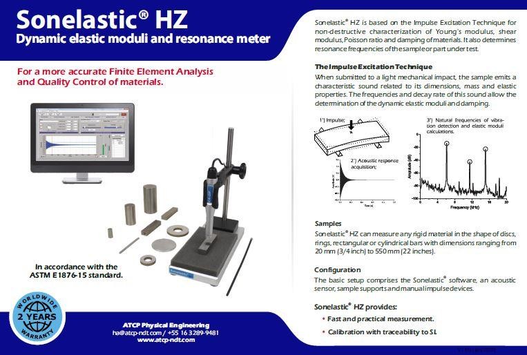
Kategorie
- Instrumentierung >> Instrumente Zum Messen, Temperaturkontrolle >> Waren >> Thermometer, Pyrometer, Wärmebildkameras
- Instrumentierung >> Instrumente Zum Messen, Temperaturkontrolle >> Waren >> Temperatursensoren
- Instrumentierung >> Instrumente Zum Messen, Temperaturkontrolle >> Waren >> Widerstandsthermometer
Produktinformation
Auftragsvolumen ab: Auf Anfrage
Lieferbedingungen: Aufsammeln
Grundinformation
Produktbeschreibung:
Das Wafer-Messsystem ist eine hochmoderne Lösung, die speziell für die Wafer-Industrie entwickelt wurde. Es bietet eine Reihe leistungsstarker Funktionen und Fähigkeiten, um genaue und präzise Messungen sicherzustellen.
Hier sind die Hauptmerkmale des Wafer-Messsystems:
1. Messtechnik: Verwendet einen berührungslosen Koaxial-Laser-Wegsensor vom Wegmesstyp für präzise Messungen.
2. Gantry-Bewegungsmechanismus: Ausgestattet mit einem hochpräzisen Linearmotor-Gantry-Bewegungsmechanismus, der reibungslose und genaue Bewegungen während der Messungen gewährleistet.
3. Kompatibilität: Entwickelt, um sowohl polierte als auch unpolierte, transparente und nicht transparente Wafer zu messen, wodurch es für verschiedene Anwendungen vielseitig einsetzbar ist.
4. Wafergrößenkompatibilität: Unterstützt Waferproben mit einem Durchmesser von 1 bis 8 Zoll, mit der Option, die Kapazität auf größere Produkte mit 300 mm (12 Zoll) zu erweitern.
5. Verbesserte Stabilität: Enthält ein koplanares, luftschwebendes, mobiles Lagersystem, das sicherstellt, dass sich die Waferprobe mit außergewöhnlicher Ebenheit und Sanftheit bewegt und mögliche Störungen minimiert.
6. Messbereich: Kann die Dicke eines Wafers im Bereich von 10 Mikrometern bis 20 Millimetern messen und ist für einen breiten Bereich an Waferdicken geeignet.
7. Maximale Scangeschwindigkeit: Bietet eine schnelle Scangeschwindigkeit von bis zu 1 Mikrometer pro Sekunde und ermöglicht so effiziente und zeitsparende Messungen.
8. Messparameter: Bietet umfassende Messparameter, einschließlich Dicke, Gesamtdickenschwankung (TTV), lokale Dickenschwankung (LTV), Gesamtindikatorwert (TIR), Sori, Konizität, Biegung und Warp. Bei diesen Messungen werden die Industriestandards eingehalten.
Das Wafer-Messsystem ist ein unverzichtbares Werkzeug für die Wafer-Industrie und ermöglicht präzise und genaue Messungen verschiedener Wafer-Eigenschaften. Ob für Forschung und Entwicklung oder zur Qualitätskontrolle, dieses System bietet Zuverlässigkeit, Vielseitigkeit und Effizienz bei Wafermessungen.


