
 Unternehmen


 Unternehmen
 Geschäft
 Gewerbeimmobilien
 Investition
 Franchise
 Ausrüstung
 Sonderausstattung
 Waren
Waren
 Dienstleistungen
 Ausschreibungen
 Dienstleistungen für Arbeitgeber
 Dienstleistungen für Arbeitssuchende
 Angebote veröffentlichen
 Aufnahme in das Firmenverzeichnis
 Professionelle Pakete
 Dienstleistungen für Arbeitgeber
 Dienstleistungen für Stellensuchende/Freiberufler

3727
China, Beijing Stadt, Beijing - siehe genauen Standort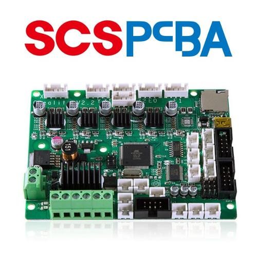
Kategorie
Produktinformation
Auftragsvolumen ab: Auf Anfrage
Lieferbedingungen: Aufsammeln
Grundinformation
Die Leiterplattentrennung ist ein entscheidender Schritt in der Elektronikfertigungsindustrie, insbesondere bei der Produktion großer Baugruppen. Um die Effizienz von PCB- und SMT-Produktionslinien zu optimieren, entwerfen Ingenieure Leiterplatten häufig so, dass sie aus mehreren kleineren Einzelplatinen bestehen, die zusammen als Panel oder Multiblock bezeichnet werden. Diese Panels werden dann einem Depanelisierungsprozess unterzogen, um sie in einzelne Leiterplatten zu trennen.
Die Depanelisierung findet typischerweise in verschiedenen Phasen des Herstellungsprozesses statt, abhängig von den spezifischen Anforderungen des Endprodukts. Dies kann direkt nach dem SMT-Prozess, nach dem In-Circuit-Test (ICT), nach dem Löten von Durchgangslochkomponenten oder sogar kurz vor der endgültigen Montage der PCBA im Gehäuse auftreten.
Durch die Aufteilung des größeren Panels in einzelne Leiterplatten wird der Herstellungsprozess rationalisiert, was einen verbesserten Durchsatz und eine höhere Effizienz ermöglicht. Die Leiterplatten-Nutzentrennung spielt eine entscheidende Rolle bei der Gewährleistung einer erfolgreichen Elektronikmontage und ist ein wesentlicher Schritt bei der Herstellung hochwertiger, zuverlässiger Produkte.


