 Negocio


 Negocio
 Negocio
 Propiedad comercial
 Inversiones
 Franquicia
 Equipo
 Equipamiento especial
 Bienes
 Servicios
 Licitaciones
 Servicios para empleadores
 Servicios para buscadores de empleo
 Publicación de listados
 Colocación en el directorio de empresas
 Paquetes profesionales
 Servicios para empleadores
 Servicios para buscadores de empleo/autónomos

Montaje de placas de circuito impreso (PCB) personalizadas
China, Ciudad de Shanghai, Llevar a la fuerza - ver ubicación exacta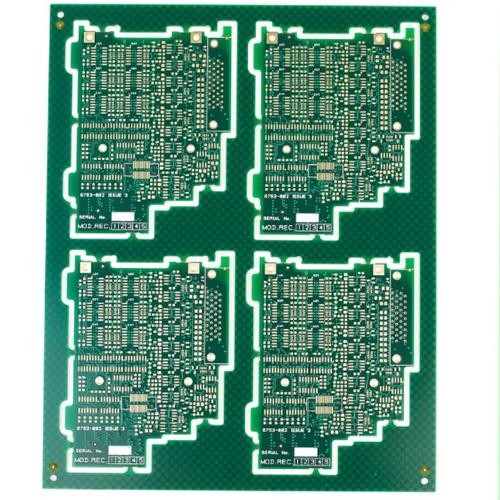
Categoría
Información del producto
Volumen de pedidos desde: Bajo pedido
Terminos de entrega: Recoger
Información básica
PCB depanelization is a critical process in the electronics industry that facilitates the production of large-scale assemblies. In the manufacturing of printed circuit boards (PCBs) and surface mount technology (SMT), the throughput of production lines can be significantly enhanced by designing PCBs as clusters, consisting of smaller individual boards intended for use in the final product.
These panel or multi-block clusters are subsequently subject to a depanelization process, whereby the large panel is broken down. The timing of this operation varies depending on the specific product requirements. In some cases, depanelization occurs right after the SMT process, while in other instances, it may follow the in-circuit test (ICT), soldering of through-hole components, or even take place just prior to the final assembly of the printed circuit board assembly (PCBA) in the enclosure.
By effectively executing the PCB depanelization process, manufacturers can optimize the production flow, achieve higher productivity, and ensure the proper functioning of the final electronic products.