 Entreprise


 Entreprise
 Entreprise
 Propriété commerciale
 Investissement
 Franchise
 Équipement
 Matériel lourd
 Des biens
 Prestations de service
 Appels d'offres
 Services aux employeurs
 Services aux demandeurs d'emploi
 Publier des annonces
 Placement dans l'annuaire des entreprises
 Forfaits professionnels
 Services aux employeurs
 Services aux demandeurs d'emploi/indépendants

Montage de carte de circuit imprimé personnalisée
Chine, Ville de Shanghai, Shanghai - voir l'emplacement exact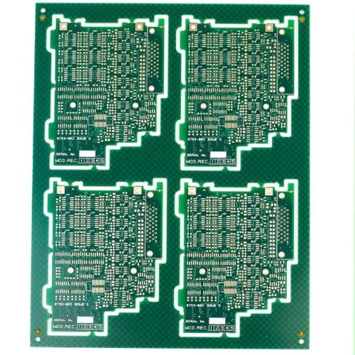
Catégorie
- Composants Pour Ordinateurs Et Ordinateurs Portables >> Ordinateurs Et Logiciels >> Des biens >> Câbles et connecteurs
- Composants Pour Ordinateurs Et Ordinateurs Portables >> Ordinateurs Et Logiciels >> Des biens >> Cartes mères
- Composants Pour Ordinateurs Et Ordinateurs Portables >> Ordinateurs Et Logiciels >> Des biens >> Autres composants
Information sur le produit
Volume de commande de: Sur demande
Conditions de livraison: Ramasser
Informations de base
PCB depanelization is a critical process in the electronics industry that facilitates the production of large-scale assemblies. In the manufacturing of printed circuit boards (PCBs) and surface mount technology (SMT), the throughput of production lines can be significantly enhanced by designing PCBs as clusters, consisting of smaller individual boards intended for use in the final product.
These panel or multi-block clusters are subsequently subject to a depanelization process, whereby the large panel is broken down. The timing of this operation varies depending on the specific product requirements. In some cases, depanelization occurs right after the SMT process, while in other instances, it may follow the in-circuit test (ICT), soldering of through-hole components, or even take place just prior to the final assembly of the printed circuit board assembly (PCBA) in the enclosure.
By effectively executing the PCB depanelization process, manufacturers can optimize the production flow, achieve higher productivity, and ensure the proper functioning of the final electronic products.